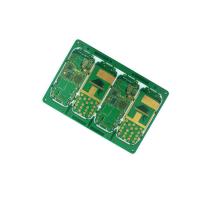
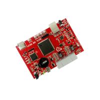
PTFE PCB Layout Design Mixed Voltage Embedded Capacitor Carbon Ink
PCB Layout Design Description:
1. Focus on component sourcing.
2. Management team with 10+ years of experience in the material.
3. PCB Component Sourcing Teams: Project department, Engineering
department, Purchasing.
4. department, Quality department, Customs Declaration department.
5. Professional component validation engineers.
6. Professional BOM Engineers.
PCB Layout Design Parameters:
| Item | Technical Parameter |
| Layer | 2-64 |
| Thickness | 0.5-17.5mm |
| Copper Thickness | 0.3-12 oz |
| Min Mechanical Hole | 0.1mm |
| Min Laser Hole | 0.075mm |
| HDI | 1+n+1,2+n+2,3+n+3 |
| Max Aspect Ratio | 20:01 |
| Max Board Size | 650mm*1130mm |
| Min Width/Space | 2.4/2.4mil |
| Min Outline Tolerance | ±0.1mm |
| Impedance Tolerance | ±5% |
| Min PP Thickness | 0.06mm |
| Bow &Twist | ≤0.5% |
| Materials | FR4,High-Tg FR4,Rogers, Nelco,RCC,PTFE, M4, M6,TU862,TU872 |
| Surface Finished | HASL, HASL Pb Free Immersion Gold/Tin/Silver Osp, Immersion
Gold+OSP |
| Special Capability | Gold Finger Plating, Peelable, Carbon ink |
PCB Layout Design Introduction:
1. Under normal circumstances, all components should be arranged on
the same side of the circuit board. Only when the top components
are too dense, can some devices with limited height and low heat
generation, such as chip resistors, chip capacitors, Chip IC, etc.
are placed on the bottom layer.
2. On the premise of ensuring electrical performance, components
should be placed on the grid and arranged in parallel or
perpendicular to each other to be neat and beautiful. In general,
components are not allowed to overlap; the arrangement of
components should be compact, and components should be placed on
the entire layout. The distribution is uniform and the density is
consistent.
3. The minimum spacing between adjacent pad patterns of different
components on the circuit board should be more than 1MM.
4. The distance from the edge of the circuit board is generally not
less than 2MM. The best shape of the circuit board is a rectangle,
and the aspect ratio is 3:2 or 4:3. When the surface size of the
circuit board is greater than 200MM by 150MM, it should be
considered that the circuit board can withstand Mechanical
strength.


